Laser-embedded nanosilver conductors

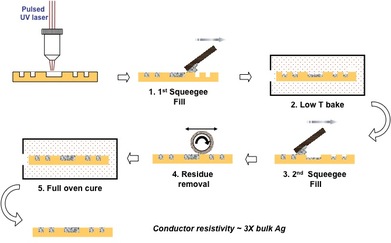
Nano-silver conductor fabrication process.
Conductor width as small as 10 microns.
Our embedded conductors with widths as small as 10 microns are fabricated using nanoparticle silver pastes. They allow us to easily route traces between pads and build interconnect structures with a minimal number of layers. This reduces fabrication cost and enhances yield and reliability. The laser patterning process also allows a high degree of control over depth of the embedded conductors and enhances substrate adhesion. Embedded conductors can be produced in a variety of substrate materials.
Green, lead-free fabrication
There is no use of metal plating or etching processes.
Compatible with rapid prototyping and small batch fabrication
All substrate fabrication steps can be defined by a single CAD drawing, and no masks are required.
A whitepaper describing fabrication of Single and Double Layer Circuits with Embedded Nanoparticle Conductors is available on the Downloads page.